
Products
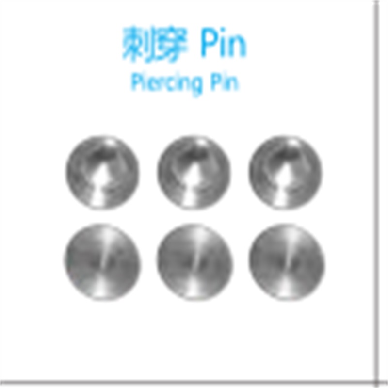


PCB Piercing Pin
Five Advantages Of Products
- Exposure optical imaging graphic transfer special positioning nails in double/multi-layer printed circuit board.
- Pointed end.
- Four sides open.
- -
- -
Product Details
PCB Piercing Pin
USAGE
Exposure optical imaging graphic transfer special positioning nails in double/multi-layer printed circuit board.
CHARACTERISTICS
Pointed end, four sides open.
TOLERANCE
+0.005mm/-0.02mm
SPECIFICATION
Φ5.0×1.2×Φ3.1,
Φ5.0×1.5×Φ3.0,
Φ5.0×1.5×Φ3.15,
Φ6.0×1.4×Φ3.1,
Φ6.0×1.45×Φ3.15,
Φ6.0×1.45×Φ3.175
WEHANS AUTOMATION TECHNOLOGY. CO., LTD
Contact Person: Cynthia
Telephone: +86 15062667823
Landline: +86 18121053868

Company Address: Building 1, No. 268, Dengyun Road, Yushan Town, Kunshan City, JIangsu Province, China.
Website: www.wehans-tech.com
Previous: PCB Silk Screen Copper Pin
Inquiry :

-
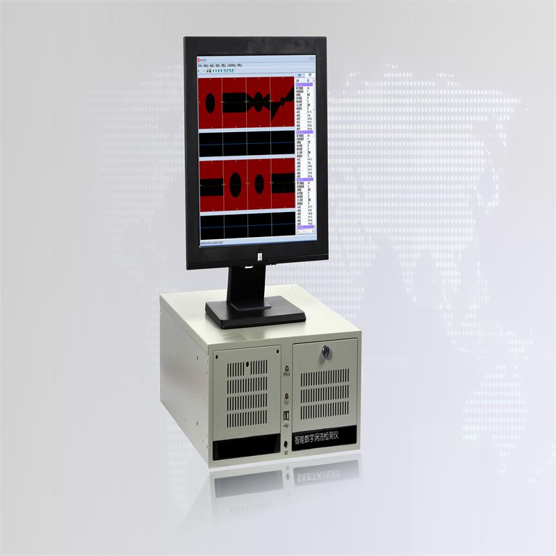
Multi-channel intelligent digital eddy current detector EIG3000
-
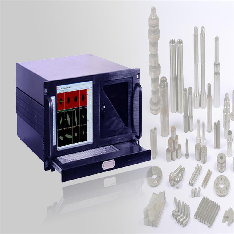
Multi frequency& multi-channel intelligent digital eddy current detector EK3000
-
Multi-channel intelligent digital eddy current detector EIG2000
-
Intelligent digital eddy current material sorting instrument ERS6000
-

On-line eddy current testing system for stainless steel straight welded pipe ECN1002/EFN1002
-

On-line eddy current testing system for straight welded pipe EFH1002
-
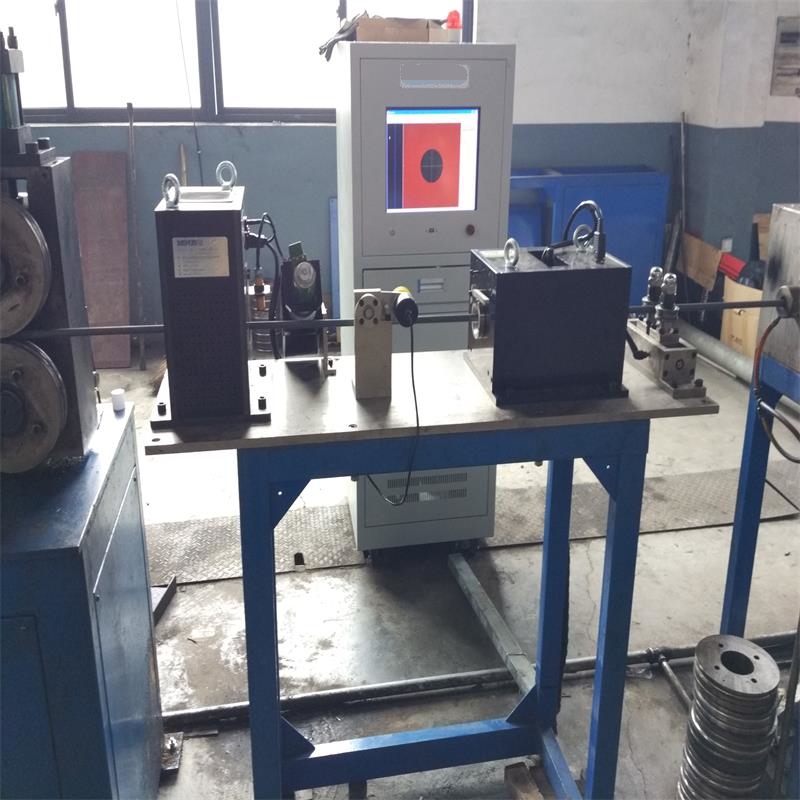
On-line eddy current testing system for spring steel wire ECH7002
-
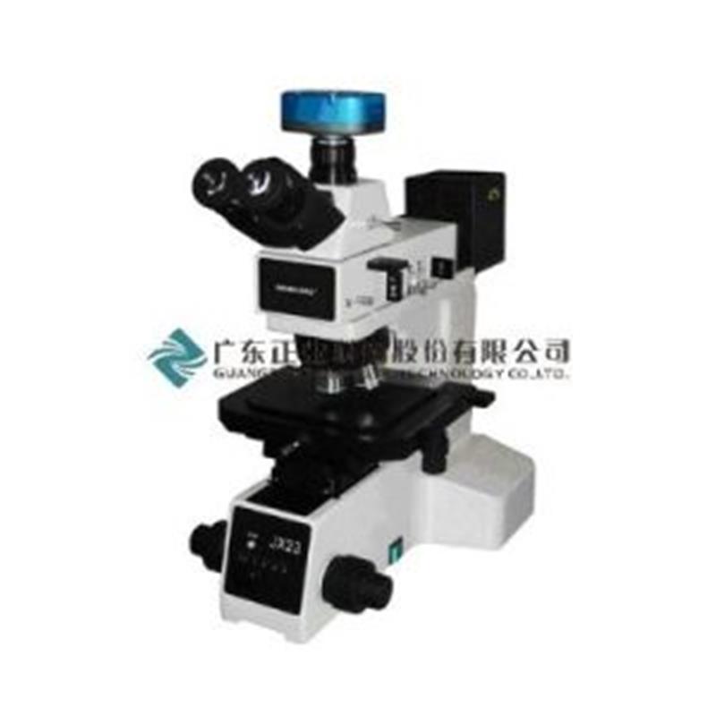
PCB Metallographic Microscope (JX22/JX23-RT)